Verilog 阻塞赋值与非阻塞赋值(二)
时间:2021-03-15 11:35:38
收藏:0
阅读:0
问题一
在这个程序下:
//d=a+b
//out=d+c

always @(posedge Clk or negedge Rst_n) begin
    if(!Rst_n)
        out = 2‘b0;
    else begin
        d <= a + b;
        out <= d + c;
    end

end
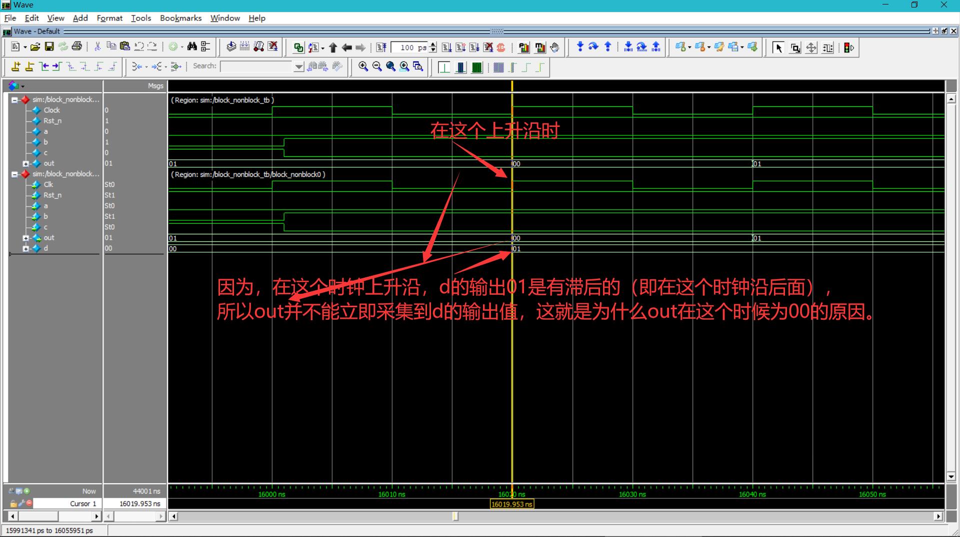
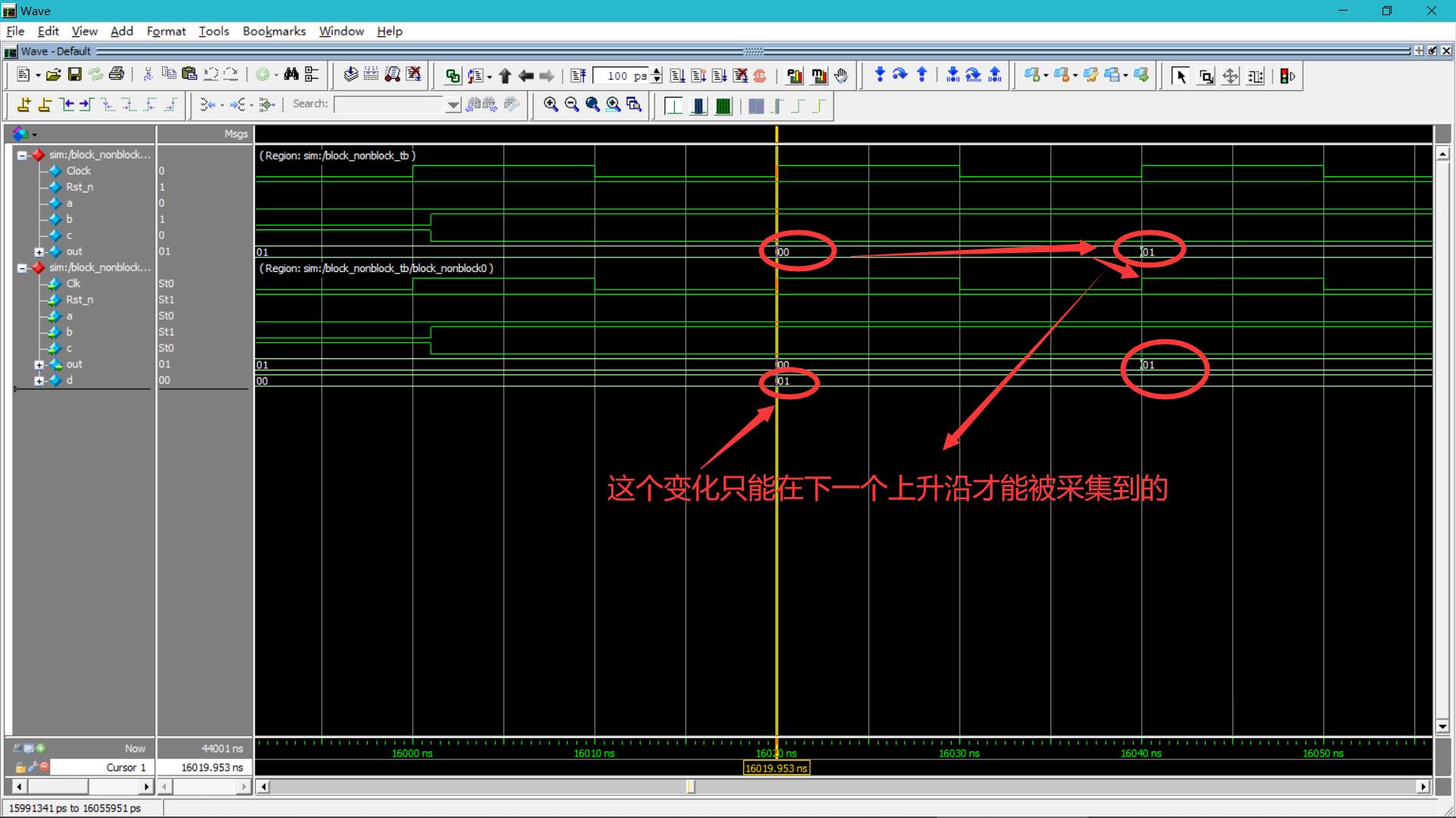
- 问题:出现了out暂时为00的情况;即d被赋值的同时out没有被赋值
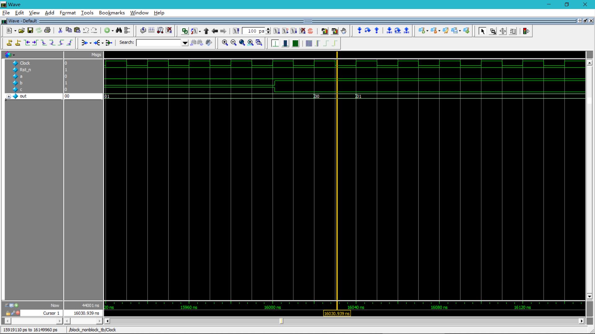
问题分析:分析出现了out暂时为0的情况
分析出现了out暂时为0的情况(2):
-
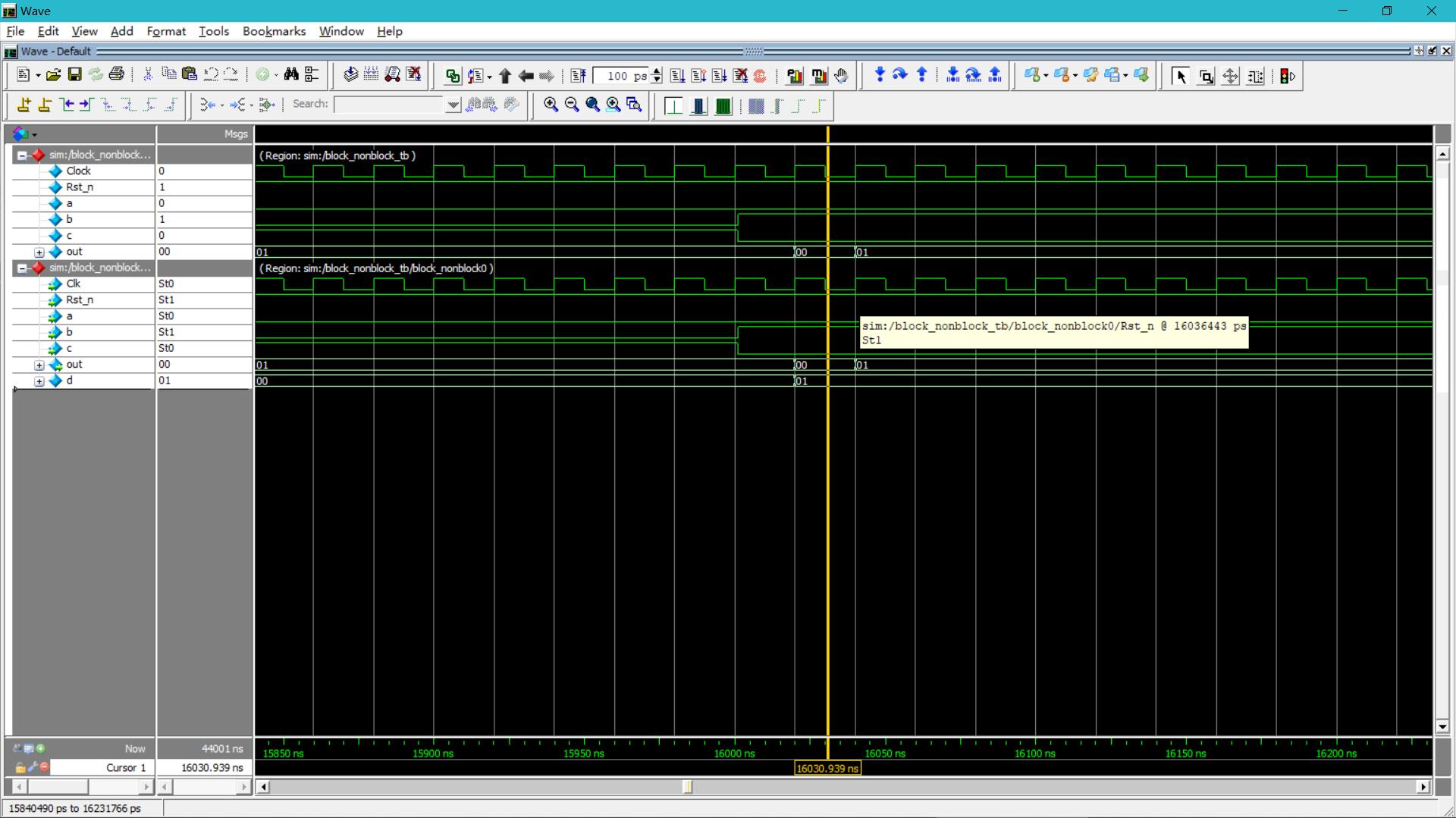
上面这种仿真是功能仿真,不太好理解,下面模拟下电路延迟就好理解了;
-
加上了“模拟电路延迟”后的程序如下:
`timescale 1ns/1ns
`define tp 1
module block_nonblock(Clk,Rst_n,a,b,c,out);

    input Clk;
    input Rst_n;
    input a,b,c;

    output reg [1:0]out;
//因为out 是在always@ 中进行赋值的,所以要将out定义为reg类型

//  out = a + b + c; //把该算式分解为两步
//  d = a + b;
//  out = d + c;
    reg [1:0]d;

always @(posedge Clk or negedge Rst_n) begin
    if(!Rst_n)
        out <=#`tp 2‘b0;		//加入模拟电路延迟
    else begin
        d <=#`tp a + b;
        out <=#`tp d + c;
    end

end

endmodule
- 仿真波形如下
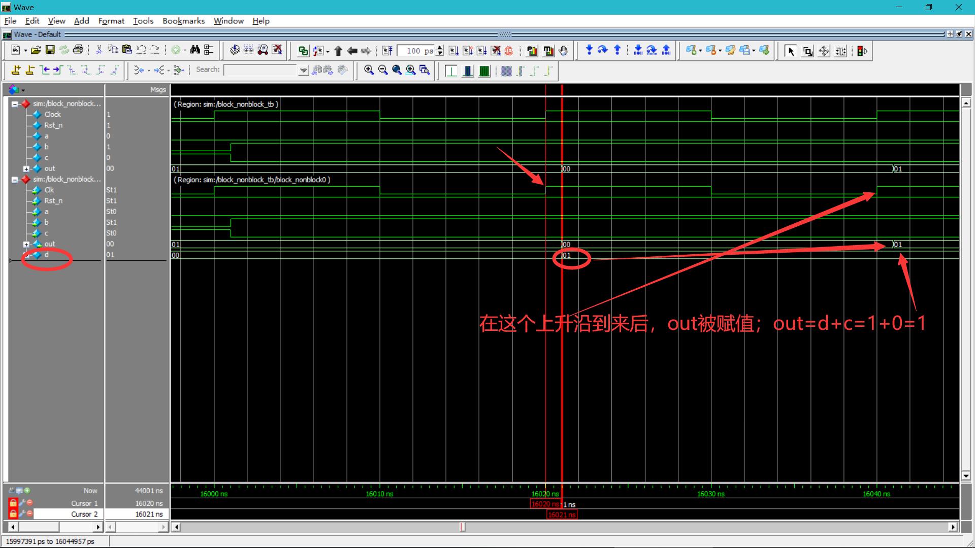
现在可以明确的看到,当时钟上升沿检测到b=1,a=0的时候,就会对d进行赋值操作,但这样一个赋值操作并不是马上就发生的,而是之后了这么久(#`tp),才对d进行的赋值,d=1;并在下一个上升延时才对out进行赋值;
在实际的电路中就是这种情况。
- 时序仿真:
程序:
module block_nonblock(Clk,Rst_n,a,b,c,out);

    input Clk;
    input Rst_n;
    input a,b,c;

    output reg [1:0]out;
//因为out 是在always@ 中进行赋值的,所以要将out定义为reg类型

//  out = a + b + c; //把该算式分解为两步
//  d = a + b;
//  out = d + c;
    reg [1:0]d;

always @(posedge Clk or negedge Rst_n) begin
    if(!Rst_n)
        out <= 2‘b0;
    else begin
        d <= a + b;
        out <= d + c;
    end

end

endmodule
时序的仿真波形如下:
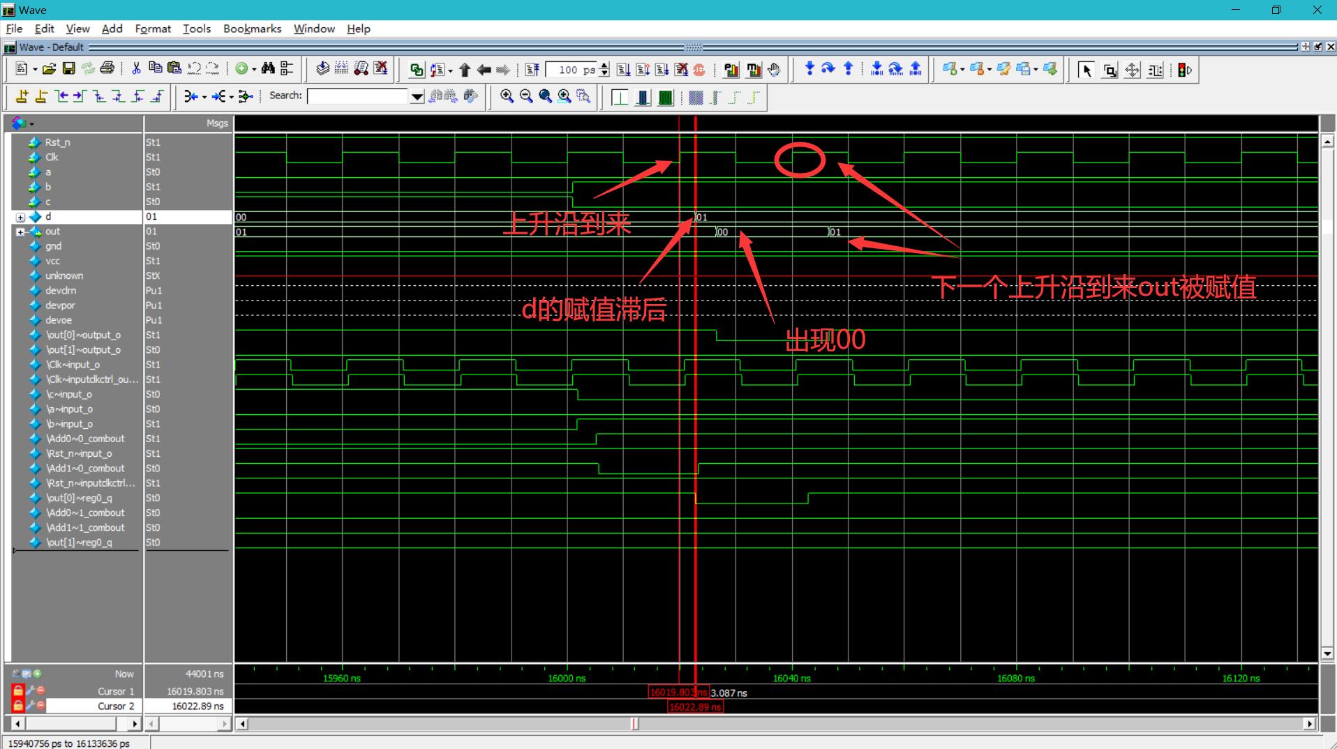
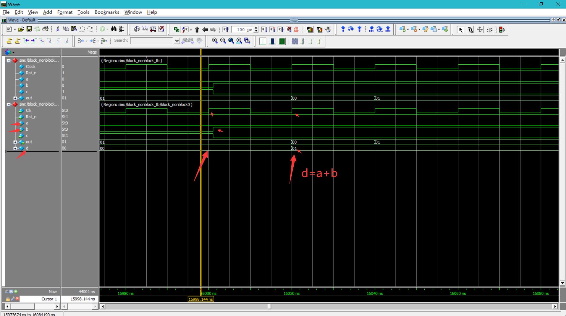
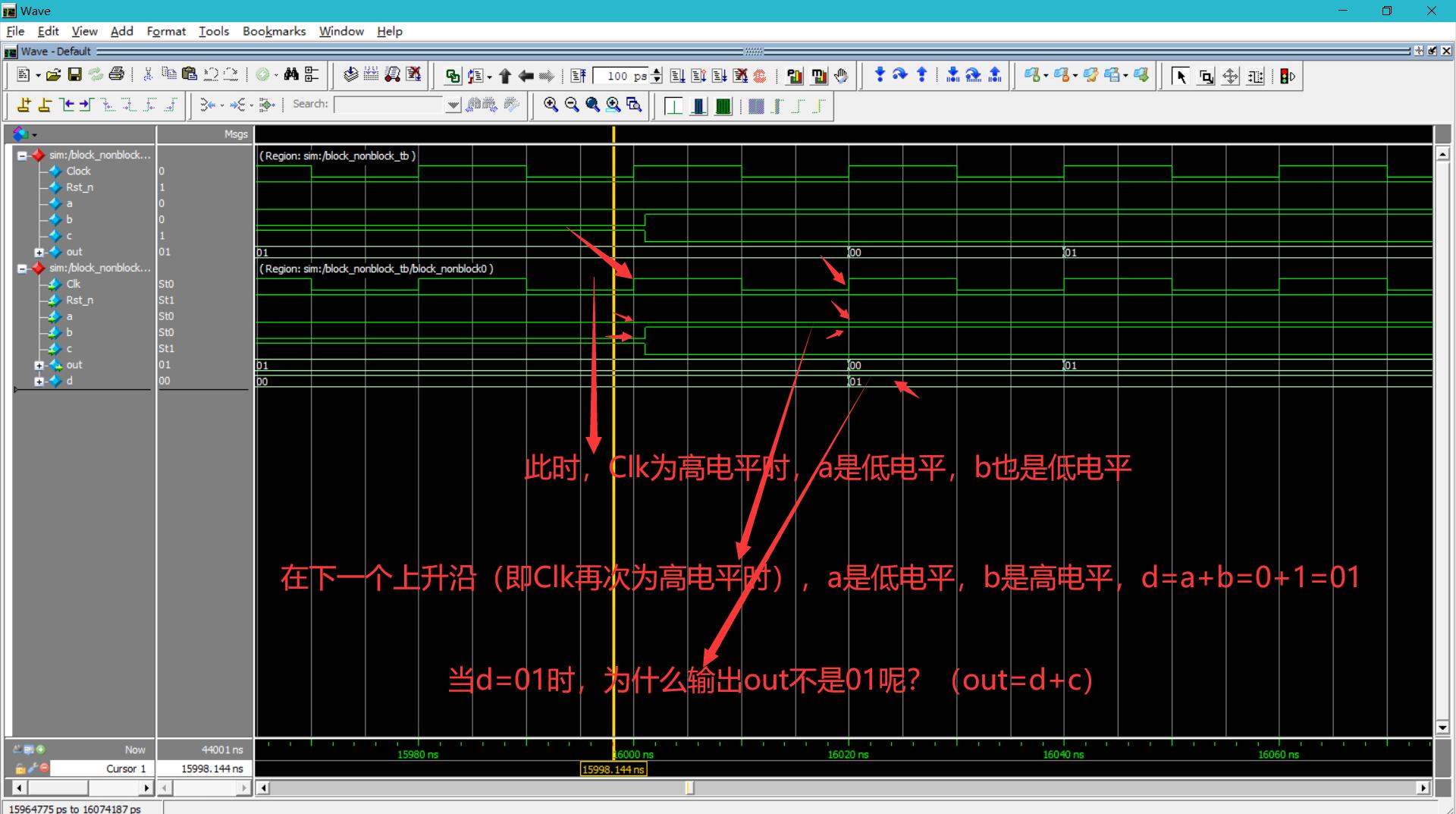
- 小结:这是非阻塞赋值中出现的一个问题,即以时钟为基准,赋值之后,这个具体的值并不是在当前时钟上升沿时进行输出的,而是在下一个时钟上升沿才会被输出;即非阻塞赋值的这两条语句
d <= a + b; out <= d + c;的执行是没有先后顺序的;也就是说out 执行时所用到的值,是前一个时钟沿其它(d 和c)数据的结果。
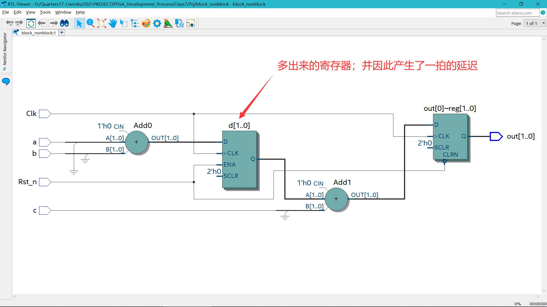
在这个过程中,out 的这个 00 的状态是我们不希望看到的;为什么这里out的值 会相比于a+b=d 的值会有一拍的的延迟呢?原因就是中间加的 这一个 d = a+b ,从而使生成的电路中多出一个寄存器(如下图),所以在always@ 语句块中推荐使用非阻塞赋值。
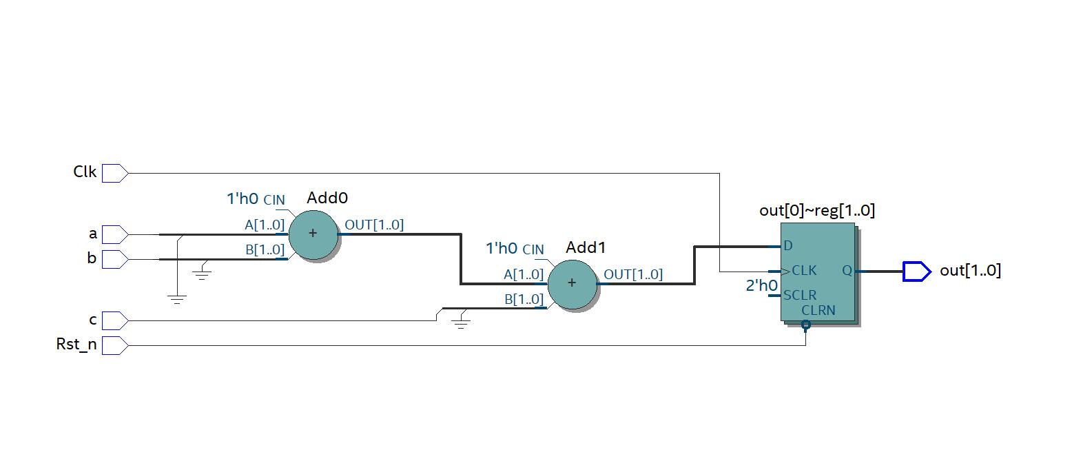
- 优化:如果想把这个寄存器去掉,即避免那一拍的延迟,可将代码做如下修改:
always @(posedge Clk or negedge Rst_n) begin
    if(!Rst_n)
        out <= 2‘b0;
     else begin
    //     d <= a + b;
    //     out <= d + c;
    out <= a + b + c;   //a+b+c是一段组合逻辑
    end

end
endmodule
生成电路如下:
评论(0)